Press Release
20 July 2023
Look for a lock (![]() ) or https:// as an added precaution. Share sensitive information only on official, secure websites.
) or https:// as an added precaution. Share sensitive information only on official, secure websites.
Designs $2 billion state-of-the-art factory to meet future demands for high-performance technology with a commitment to skilled talent
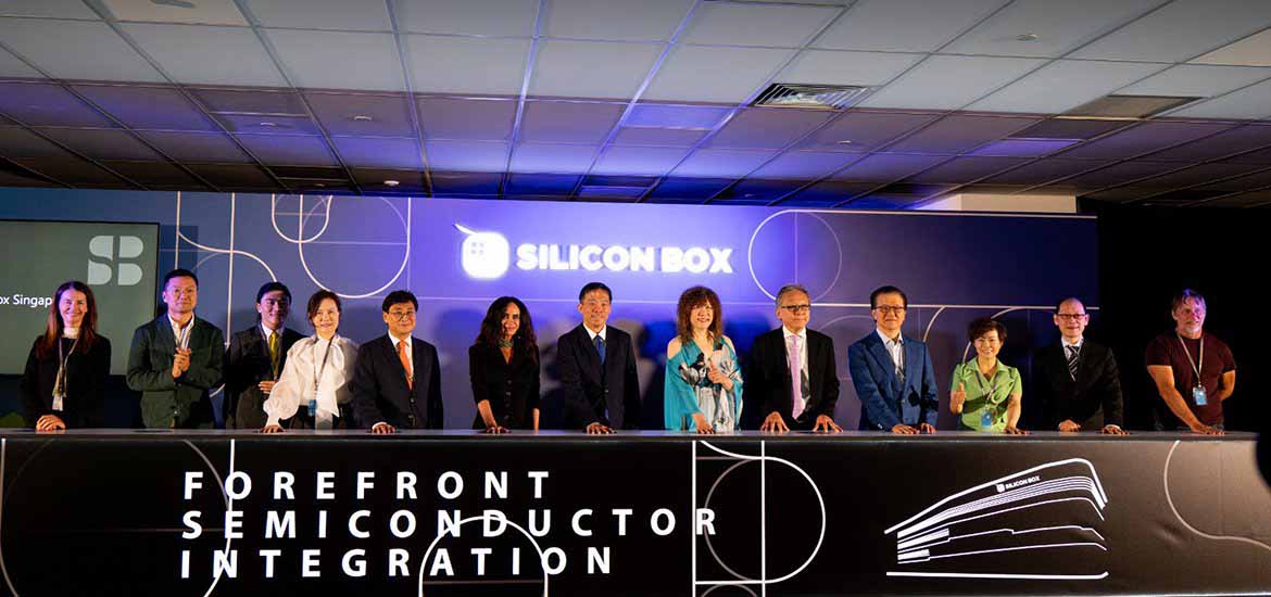
Photo credit: Silicon Box
Singapore, July 2023 – Silicon Box, a cutting-edge semiconductor heterogeneous integration startup, today unveiled its $2 billion advanced semiconductor manufacturing foundry aimed at revolutionising the chip manufacturing sector, developing local capabilities, and boosting Singapore’s position as a global hub for semiconductor manufacturing. Silicon Box will hire and train up to 1,200 high-level employees, with the support of the Singapore Economic Development Board (EDB).
The grand opening ceremony of the 73,000 sqm facility in Tampines, the size of 15 football fields, was graced by Mr Png Cheong Boon, Chairman EDB, and the company’s three co-founders Dr. Han Byung Joon - Chief Executive Officer of Silicon Box - Dr. Sehat Sutradja, and Weili Dai.
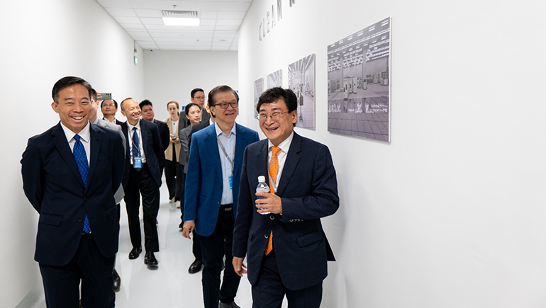
Photo credit: Silicon Box
“Silicon Box is well poised to solve the unique challenge for chiplets, which are essential to power emergent technologies. Our team of experts with over 30 years of multi-sectoral experience, critical ecosystem of partners and proprietary interconnection technology will shorten the design cycle of chiplets, lower new device costs, reduce power consumption and enable faster-time-to-market for industry partners involved in areas such as artificial intelligence (AI), data centres, electronic vehicles (EVs), mobile, and wearables, while protecting their intellectual property (IP).”
Dr. Han Byung Joon
Chief Executive Officer
Silicon Box
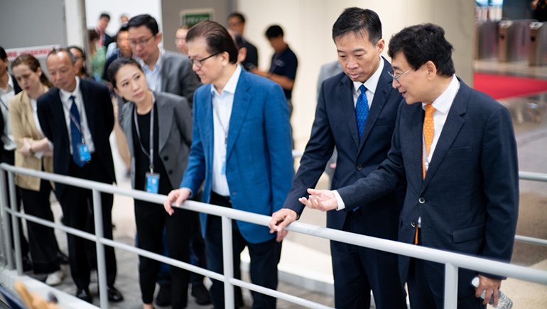
Photo credit: Silicon Box
Transforming the semiconductor industry with advanced chiplet interconnection technology
Despite its wide potential and high demand across emerging technologies, deployment of chiplets continues to face challenges with manufacturing capacity, complexity and cost. Silicon Box’s proprietary fabrication method, sets a new standard for design flexibility and electrical performance at low cost, and delivers one of the shortest interconnections using sub 5 micron technology. This agility in semiconductor design cycles enables the industry to effectively and efficiently scale across the semiconductors value chain.
Developing talent for qualitative transformation of the manufacturing sector
Digitalisation, accelerated by the pandemic, has increased demand for talent in high-end engineering. Leveraging the combined expertise and patents of the co-founders of Silicon Box and commitment to R&D, the startup aims to attract the brightest minds and digital experts to join the innovative team at the facility. In collaboration with EDB, Silicon Box will be providing training opportunities for graduates from institutes of higher learning to contribute to the development of radical new technologies to meet this demand.
Silicon Box is a Singapore-based, global champion in semiconductors that will bring the city-state to the forefront of innovation in the space. It will help facilitate further development of native supply chains and technologies for this critical industry.
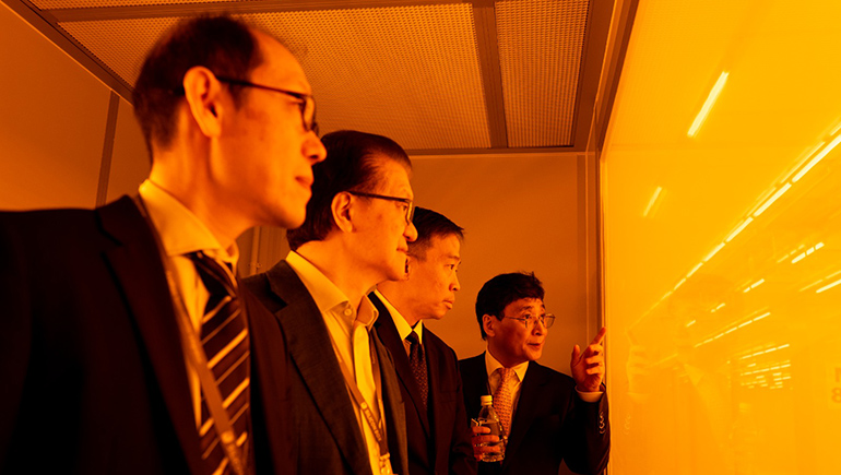
Photo credit: Silicon Box
“Singapore is home to a vibrant and sophisticated semiconductor industry, with a strong ecosystem of solution providers and partners. Silicon Box’s decision to set up its first manufacturing and R&D facility in Singapore is testament to our competitiveness as a critical global node for semiconductors, and a vote of confidence in the long-term growth prospects of the sector in Singapore. We will continue to strengthen our industry’s competitiveness by developing a stronger talent pipeline, reducing the sector’s carbon footprint and deepening our semiconductor R&D capabilities."
Png Cheong Boon
Chairman
EDB
“Silicon Box brings its cutting-edge design capabilities and propriety packaging system in chiplets to an established semiconductor ecosystem at Tampines Wafer Fab Park, where it can collaborate and build partnerships with industry players. We are pleased to support Silicon Box in the development of its purpose-built facility which will house R&D and manufacturing functions under one roof, enabling it to ramp up operations quickly and shorten time-to-market to meet customer demands.”
Cheong Wee Lee
Director, Biomedical & Electronics Cluster Group
JTC
End-to-end commitment on economic resource efficiency at scale
Operating with economically sound processes to minimise the negative effects on the environment, Silicon Box ensures that its interconnected chiplets are energy efficient at scale. Built with resource efficiency in mind in keeping with industry best practices, the facility includes:
Press Release
20 July 2023