- The fab extension will enable Soitec to double the annual production at its Pasir Ris site, in Singapore, to around two million 300mm SOI (Silicon-on-Insulators) wafers
- The production ramp-up is part of Soitec's strategic growth plan to address the increasing global demand for engineered wafers and complements its investments at its main hub in France
- The extension in Singapore will add 45,000 square meters of fab space and double Soitec’s Singapore workforce to more than 600 by 2026
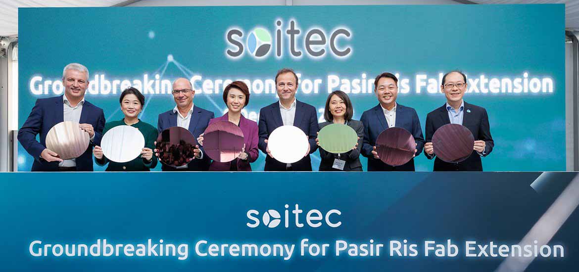
Soitec (Euronext Paris), a world leader in the design and production of innovative semiconductor materials, today formally broke ground on the construction of its wafer fab extension at Singapore’s Pasir Ris Wafer Fab Park. The ceremony was held in the presence of Low Yen Ling, Singapore’s Minister of State for Trade and Industry, and Her Excellency, Minh-di Tang, Ambassador of France to Singapore.
The fab extension will be dedicated to the production of 300mm SOI wafers, which are used to produce chips for smartphones, particularly in 5G communications, as well as vehicles and smart devices. Upon its completion in 2024, the extension will add 45,000 square meters of clean room and office space and enable Soitec to double its annual production capacity in Singapore to around two million 300mm SOI wafers.
The extension has been designed to support Soitec’s commitments to an energy-efficient use of resources and make the new facility a sustainable, state-of-the-art working environment. Soitec aims to double its workforce in Pasir Ris to more than 600 by 2026. In parallel to this extension, Soitec is also expanding its technology presence in Singapore with the operational start of its characterization Lab within Soitec’s Singapore Technology Center.
The extension of Pasir Ris in Singapore complements Soitec’s investments in France and is part of its strategy to meet the increasing demand by ramping up its global annual production capacity to around 4.5 million wafers by fiscal year 2026. This includes a wide range of specialized energy-efficient wafers, using different materials (Silicon-on-Insulator, Gallium Nitride, Piezoelectric-on-Insulator and Silicon Carbide) and to serve different markets. Soitec’s investments in Singapore and France are part of a five-year €1.1bn capital expenditure program announced in June 2021.